
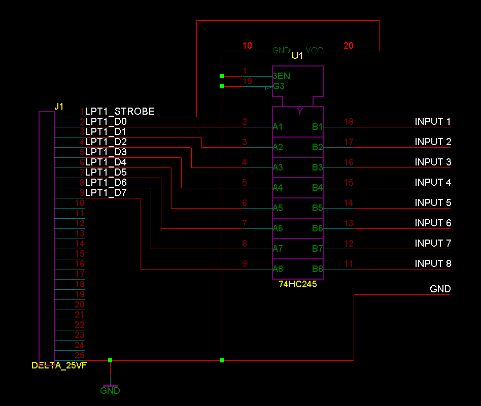
Original circuit diagram
The TFLA is a 8 port logic analyzer. Connected to the parallel port of a fast PC, the sampling rate can reach 1 MHz, And that makes it usable for my 6502 systems! Also perfect to analyze serial transmission.
I have built the TFLA, the acronym for The Fabulous Logic Analyzer.
Not my own design, here is the original design, here the Windows program and here the source and design.
The TFLA is a 8 port logic analyzer. Connected to the parallel port of a fast PC, the sampling rate can reach 1 MHz, And that makes it usable for my 6502 systems! Also perfect to analyze serial transmission.
I made some changes to the original design:
– Between the parallel port and the output of the buffer I added 1 K resistors. To protect PC ports that are not bidirectional.
– Added 100 ohm resistors between the input and the buffer. To protect the buffer.
– Added 10k ohm resistors to ground at the input of the buffer. This makes sure an unconnected input is at null level.
– Power for the buffer IC is taken from the USB port. Also this +5V is brought to the outside, enough to provide power for experiments.
– The buffer is a 74HCT245, a perfect low power high impedance buffer IC.
– Connection between the TFLA and the parallel port via a Centronics connector (from an old printer!) and a standard printer cable.
– The connectors for the logic input signals are from Conrad (2.6 mm) 730599 – 89 and 733628 – 89 (PCB bus).
– The clips are from dealextreme.com
– The simple circuit is built on a strip-board.
Here are the photos:


